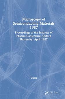
Microscopy of Semiconducting Materials 1987, Proceedings of the Institute of Physics Conference, Oxford University, April 1987
A.G. Cullis
Jan 2021 · CRC Press
Ebook
820
Pages
family_home
Eligible
info
reportRatings and reviews aren’t verified Learn More
About this ebook
The various forms of microscopy and related microanalytical techniques are making unique contributions to semiconductor research and development that underpin many important areas of microelectronics technology. Microscopy of Semiconducting Materials 1987 highlights the progress that is being made in semiconductor microscopy, primarily in electron probe methods as well as in light optical and ion scattering techniques. The book covers the state of the art, with sections on high resolution microscopy, epitaxial layers, quantum wells and superlattices, bulk gallium arsenide and other compounds, properties of dislocations, device silicon and dielectric structures, silicides and contacts, device testing, x-ray techniques, microanalysis, and advanced scanning microscopy techniques. Contributed by numerous international experts, this volume will be an indispensable guide to recent developments in semiconductor microscopy for all those who work in the field of semiconducting materials and research development.
About the author
A. G. Cullis (Author) , P. D. Augustus (Volume editor)
Rate this ebook
Tell us what you think.
Reading information
Smartphones and tablets
Install the Google Play Books app for Android and iPad/iPhone. It syncs automatically with your account and allows you to read online or offline wherever you are.
Laptops and computers
You can listen to audiobooks purchased on Google Play using your computer's web browser.
eReaders and other devices
To read on e-ink devices like Kobo eReaders, you'll need to download a file and transfer it to your device. Follow the detailed Help Center instructions to transfer the files to supported eReaders.


